
FPGA-384 - Pinout and wiring for Arduino.
Schematic Diagram
The board is open source hardware and the schematic diagram of the circuit is available by clicking on the image below.

Pin Out Guide.
Schematics can still be confusing, so here is the essential board pinout guide.
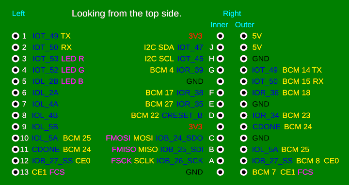
- White is board pin names.
- Black is connected ground.
- Red is connected 3V3.
- Yellow is Raspberry Pi pin names. Note that 5V is not connected as power.
- Blue is FPGA pin names.
- Mauve is board peripherals (F -> Flash IC).
A technical note about MOSI and MISO...
It is not a mistake that the Raspberry Pi MOSI is connected to the FPGA SDO pin. The Raspberry Pi is the master to both the FPGA and the Flash memory IC which are both programmed using SPI. However, when booting from Flash, then the FPGA takes on the role of being the master during the boot process. For it to drive the SPI to the Flash memory IC correctly, it is necessary to wire the FPGA SDO to Flash SI pin and the FPGA SDI to the Flash SO pin - which means that somebody is required to reverse their pins !
Therefore the Raspberry Pi must program the FPGA using IO lines and bit bashing instead of native SPI calls. The FPGA must be programmed so that it puts its SPI lines into high impedance IO mode before we assert the CS1 line to drive the Flash chip with SPI.
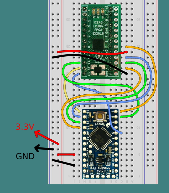
All of this has been taken care of and built into the fpga-384 utility when programming the FPGA.Wiring to an Arduino board.
The FPGA-384 board can only handle 3.3 Volt logic, so either use a 3.3 V ProMini, or use voltage level shifters.
IT IS NOT 5V TOLERANT !
Make the following connections on your breadboard:
SiliconFrog CC-BY